A common dilemma – how to figure out, which pixel pitch of the thermal imaging sensor (also known as microbolometer) suits you best: 12 or 17 microns? In other words, does size matter? A simple answer is – yes, it does. But what you should know beforehand – pixel pitch directly influences base magnification, image quality and thermal imager sensitivity. There are a lot of believes and misconceptions floating around. In this article, we will try to explain it all.
Size does matter
A common user determines the class of a thermal imaging device by the sensor resolution or, in other words, by the number of pixels horizontally and vertically. Although there are many more factors to determine the quality of a thermal image, there is a reason for this – the more pixels a sensor contains, the more details of the observed image it can show to the user.
What is thermal image quality
The resolution of a thermal imaging device is determined by the parameters of optical elements, sensor, display, design concept quality, as well as signal processing algorithms. In this article, we will consider only the influence of sensor parameters on the quality of a thermal image. As for the remaining parameters, we will proceed from the fact that they are solved in the most optimal way.
The resolution of a thermal imaging device is a complex parameter that consists of thermal and spatial resolution.
Spatial resolution characterizes the ability of a thermal imaging device to show two closely spaced dots or lines separately. The higher the resolution, the clearer the image is shown to the user. From the user's point of view, spatial resolution is the most understandable and objective parameter for determining the image quality of a thermal imaging device.
Thermal resolution (minimum detectable temperature difference) is the boundary ratio of the observed object signal to the background signal, considering the noise of a thermal imaging sensor. High thermal resolution means that a thermal imaging device can detect an object with a certain temperature against a background with a similar temperature. The smaller the difference between an object and background temperatures, which are recorded by a thermal imaging device, the higher the thermal resolution.
The most important characteristic that affects the thermal resolution of a thermal imaging device is the sensor's NETD (Noise Equivalent Temperature Difference). It is measured in millikelvins. The NETD of a sensor is a parameter that represents the smallest temperature difference that the sensor can perceive. This parameter corresponds to a signal-to-noise ratio equal to one. In other words, the change in sensor output signal at a temperature difference equal to NETD corresponds to the noise level of the sensor. The lower the NETD value, the higher the sensor sensitivity.
When choosing a thermal imaging device, customers are guided by different arguments: base magnification, detection range, field of view, weight, size, price. However, not even the most detailed technical data sheet provided by manufacturers of thermal imaging devices contains the item “image quality”. At the same time, even devices with the same field performance show noticeably different results in reality.
Let's compare two thermal imagers by Pulsar: the Axion 2 XG35 and the Helion 2 XP50 Pro
| |
Axion 2 XG35
|
Helion 2 XP50 Pro
|
|
Objective lens
|
F35/1.0
|
F50/1.0
|
|
Sensor res, pixels
|
640x480
|
640x480
|
|
Pixel pitch,
|
12
|
17
|
|
Sensor NETD, mK
|
<40
|
<25
|
|
Display resolution
|
1024x768
|
1024x768
|
|
Magnification, x
|
2.5 – 20
|
2.5 – 20
|
|
FOV, °
|
12.5x9.4
|
12.4x9.3
|
|
Detection range, m
|
1750
|
1800
|
|
Dimensions, mm
|
152x50x74
|
242x75x60
|
|
Weight, g
|
0.3
|
0.5
|
It is a good example of thermal imaging devices with similar field performance but different price. The Axion 2 XG35 and the Helion 2 XP50 Pro have the same sensor spatial resolution of 640x480 pixels, 2.5 – 20x magnification, as well as similar fields of view (12.5x9.4 and 12.4x9.3 degrees) and detection ranges (1750 and 1800 meters).
So, what is the reason for the 30% difference in price? The answer is the difference in image quality.
How to evaluate the quality of thermal imaging
If you go out with the Axion 2 XG35 and the Helion 2 XP50 Pro into the field on a summer evening and look through the eyepiece, only a well-trained eye will notice the difference in image quality – both devices will show approximately equal contrast and detailed images.
However, hunting rarely take place in ideal conditions and at the ideal time of a day for a thermal imaging device. The season of active hunting in Europe falls on autumn and winter, the time of wet weather with rain, fog and night frost. The difference in price becomes clear under such real conditions.
In conditions of low thermal contrast, the image in the Helion 2 XP50 Pro is more informative compared to the Axion 2 XG35. This is not a set of spots with a limited number of shades between black and white, this is a "photographic" contrast image with a large range of midtones and high-quality rendering of the target and background. The best thermal resolution of the Helion 2 XP50 Pro comes primarily from the sensor's NETD sensitivity - a good NETD is especially important for scenes with low thermal contrast when objects have approximately the same temperature. For example, landscapes.
The observation of low-contrast thermal scenes clearly demonstrates the coherence between the thermal resolution and the spatial resolution of a thermal imaging device. It would seem that in devices with the same sensor resolution (in our case, both sensors have a resolution of 640x480 pixels), the image visible on the display should be equally detailed?
No. If the thermal contrast of the scene is low, then a thermal imaging device with a lower thermal resolution (higher sensor NETD value) will show poorer detail distinction. Areas with similar but different temperatures will be shown on the display as equal, as well as they will have the same brightness and contrast in the pixel group image. In fact, this means less spatial resolution.
Thus, the spatial resolution of visible image is not constant and may decrease with the decrease in the thermal contrast of the observed scene. It seems like a paradox, but thermal imaging devices with lower sensor resolution and better sensitivity (for example, 384x288 pixel @ 17 µm / NETD < 25 mK) can show low-contrast scenes in more detail than thermal imaging devices with higher resolution but lower sensitivity (for example, 640x480 pixel @ 12 µm / NETD < 40 mK).
| |
Thermion 2 XG50
|
Thermion 2 XQ50 Pro
|
|
Objective lens
|
F50/1.0
|
F50/1.0
|
|
Sensor res, pixels
|
640x480
|
640x480
|
|
Pixel pitch,
|
12
|
17
|
|
Sensor NETD, mK
|
<40
|
<25
|
|
Display resolution
|
1024x768
|
1024x768
|
|
Magnification, x
|
3‒24
|
2.5‒20
|
|
FOV, °
|
8.8x6.6
|
12.4x9.3
|
|
Detection range, m
|
2300
|
1800
|
The sensor sensitivity doesn’t affect the detection range (it depends on the lens focus and the pixel pitch of the sensor). In our example, the Helion 2 XP50 Pro and the Axion 2 XG35 have the same detection range of a standard 1.8m tall object. However, if we talk about the qualitative characteristics of the observation range, namely the distance of recognition and identification, then with a decrease in the scene contrast (fog, rain, mist, increased humidity), the Axion 2 XG35 thermal imaging device will “lose” noticeably faster.
Bigger pixel better quality
Let's get back to the examples. In each of the cases considered, the best image quality was shown by devices with a sensor with a NETD <25 mK, both sensors have a pixel pitch of 17 microns.
|
Thermal Monocular
|
Axion 2 XG35
|
Helion 2 XP50 Pro
|
|
Sensor resolution, pixels
|
640x480
|
640x480
|
|
Sensor NETD, mK
|
<40
|
<25
|
|
Pixel pitch, µm
|
12
|
17
|
NETD of the sensor
The larger the pixel and the larger its area, the more LWIR radiation it is able to receive and the higher the sensitivity of the entire thermal imaging sensor. The effect of sensor size on NETD underlies the very ideology of sensors with one or another pixel size.
This is clearly seen in our example. The sensors have the same resolution, 640x480 pixels, but the sensor of the Helion 2 XP50 Pro thermal imaging device has a larger pixel size (17 microns vs. 12 microns) and finally a better sensitivity (NETD <25 mK vs. NETD <40 mK).
As a result, the Helion 2 XP50 Pro is a professional level device. By purchasing this thermal imaging device, the customer pays not only for top image quality, but also for the confidence that the device will cope with any surprises that the weather can bring during the hunting.
A few words about the advantages of sensors with a small pixel size. Firstly, for thermal imaging devices with a sensor with a smaller pixel, the same detection range, magnification, and field of view can be achieved with lenses with a smaller focus. This is what the Axion 2 XG35 showed.
In a pair of the Axion 2 XG35 and the Helion 2 XP50 Pro, both devices have the same detection range. The Axion uses a lens with a smaller focus (F35/1.0), the Helion – with a larger focus (F50/1.0), but the detection range of the devices is the same due to the smaller pixel in the Axion sensor. Under ideal conditions with the deterioration of thermal contrast at the observation site, the Helion 2 XP50 Pro will show better results as a device with the best NETD sensor.
Secondly, for the same resolution, a sensor with a smaller pixel size will have a smaller physical size. So, the device based on it can be made more compact.
What is beyond the numbers
If we compare a modern 12-micron sensor and a sensor of the early 21st century with a pixel of 25 microns, then the NETD of the first one will quite possibly be higher, since over 20 years there has been a serious progress in the development of micro bolometric sensor manufacturing technologies and the quality of materials used.
In modern sensors, the larger the pixel size, the higher the sensitivity (the NETD index is lower). This is an axiom – with the same materials, it is impossible to create a thermal imaging sensor with a smaller pixel size, lower price and at the same time better sensitivity.
The NETD of the sensor is measured in compliance with the regulations, which are the same or similar for all manufacturers. But recently, there has been a transformation of NETD from a special technical characteristic into a popular tool for promoting devices, which is not always conscientious.
Now, the best production batches of sensors with a pixel pitch of 17 µm achieve NETD less than 25 mK, with a pixel pitch of 12 µm – less than 40 mK. At the same time, there are always a certain number of sensors with a lower NETD value in the batch. This means that manufacturers can assemble a small number of high-sensitivity thermal imaging devices that are used as demonstration samples when market launch. However, such a sensitivity cannot be maintained in the manufacture of any significant production batches of devices. At the same time, in advertising and informational materials about the product, the overestimated sensitivity is declared throughout the entire life cycle.
When writing technical specifications in the device certificate, some manufacturers are guided by the parameters of market leaders and indicate the numbers that a potential consumer wants to see. As a result, today on the market you can find devices with a NETD value less than 25 mK declared for sensors with a 12-micron pixel (for example, for a sensor 640x512 @12µm), which is not true.
Some manufacturers use and take into account signal post-processing, such as image filtering, to increase NETD value. The result obtained in this way cannot be considered as the NETD value of the sensor. More correctly, it is the NETD value of a thermal imaging device and looks nice on paper. In reality, improving the NETD (i.e., reducing the value of the parameter) due to image filtering leads to a decrease in the spatial resolution of the image visible on the display, as well as to the loss of image detail and its low information value.
In the development of sensors and thermal imaging devices, there are objective laws and limitations that cannot be bypassed. A top thermal imaging device cannot be cheap. If thermal imaging devices similar in terms of declared field and functional capabilities have a significant difference in price, then it is highly probable that a low price in a more affordable device is achieved due to compromises in terms of image quality. This should be kept in mind when choosing a thermal imaging device.
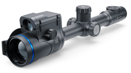 Thermion 2 LRF XL50
Thermal Imaging Riflescope
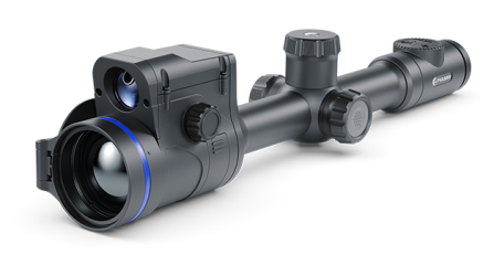 Thermion 2 LRF
Thermal Imaging Riflescopes
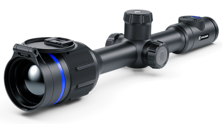 Thermion 2
Thermal Imaging Riflescopes
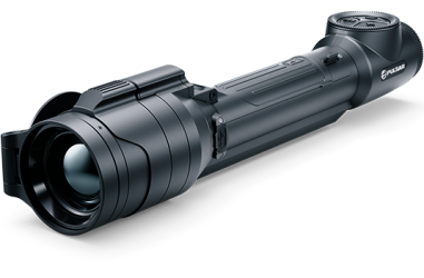 Talion
Thermal Imaging Riflescopes
New
 Merger LRF XT50
Thermal Imaging Binoculars
 Merger LRF XL50
Thermal Imaging Binoculars
 Merger LRF XP50
Thermal Imaging Binoculars
New
 Merger LRF XP35
Thermal Imaging Binoculars
 Merger LRF XQ35
Thermal Imaging Binoculars
New
 Telos
Thermal Imaging Monoculars
New
 Axion Compact
Thermal Imaging Monoculars
 Axion 2 LRF
Thermal Imaging Monoculars
 Axion 2
Thermal Imaging Monoculars
New
 Axion XQ30 PRO
Thermal Imaging Monoculars
 Krypton 2
Thermal Imaging Monocular
 Axion XM30F
Thermal Imaging Monoculars
 APS Batteries
Battery Packs
 APS Chargers
Battery Chargers
 LPS 7i Battery Pack
Battery Packs
 Telos LRF Tripod Adapter
Pulsar Accessories
 IPS Batteries
Battery Packs
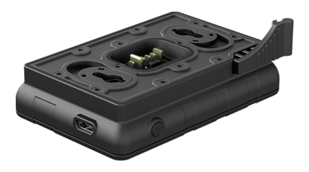 IPS Battery Charger
Battery Charger
New
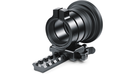 PSP-V Weaver Rail Adapter
Adapter
New
 PSP-B Ring Adapters
Ring Adapters
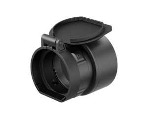 FN Adapters
Cover Ring Adapters
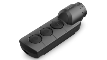 Remote Controls
for digital devices and thermal imagers
 Tree mount
Pulsar Accessories
 Window Frame Mount
Pulsar Accessories
 Flat Glass Mount
Pulsar Accessories
 Neck Straps
Accessories
New
 Monocular Pulsar 3x20 B
Accessories
 Thermal Zeroing Targets
Accessories




 English
 German
 French
 Spanish
 Italiano
 English
 Lietuvių